As modern electronics continue to evolve toward smaller form factors with higher processing power, engineers are facing growing challenges in managing electromagnetic interference, signal integrity, and thermal performance within increasingly complex layouts. The new solution portfolio is engineered to directly address these issues through an integrated approach that combines EMI shielding, RF shielding, microwave absorption, and thermal interface technologies.
High-density printed circuit boards present unique design obstacles due to tighter component spacing, faster signal speeds, and elevated heat generation. In these environments, unwanted emissions and susceptibility to external interference can significantly impact device performance and regulatory compliance. The newly introduced technologies provide targeted methods to reduce EMI on a PCB, suppress radiated and conducted noise, and maintain consistent grounding across multilayer board structures without increasing overall board thickness or weight.
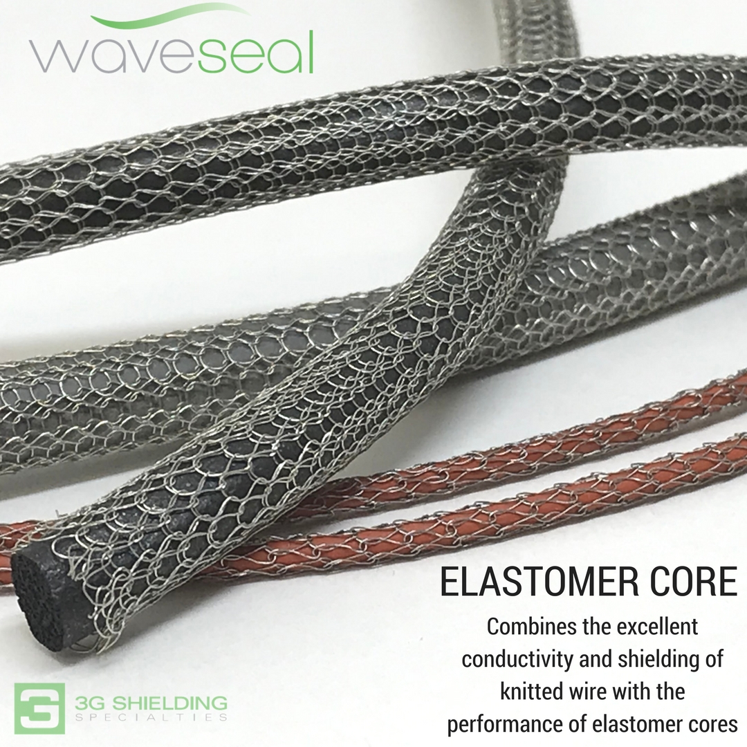
The advanced solution suite includes precision-formed board-level shields, conductive EMI gaskets, micro-profile enclosure shielding components, and hybrid absorber materials engineered for high-frequency performance. By combining conductive elements with selective RF absorbers and microwave absorbers, engineers can apply both reflective and absorptive techniques to control interference across multiple frequency ranges. This dual-strategy approach is particularly effective in environments where traditional shielding alone is insufficient to manage high-speed data transmission and complex electromagnetic interactions.
Understanding what EMI shielding is and how it works has become increasingly important for electronics manufacturers striving to meet global compliance standards. EMI shielding functions by blocking or redirecting electromagnetic waves through conductive barriers and grounding pathways, while absorber materials convert excess electromagnetic energy into minimal heat. The newly launched solutions enable engineers to implement these principles at both the board level and enclosure level, creating a comprehensive interference management ecosystem that supports consistent performance in demanding operational conditions.
In addition to electromagnetic control, the product line emphasizes integrated thermal management. Designers frequently search for the best thermal interface materials for electronic cooling as heat buildup can amplify electrical noise and degrade circuit reliability. The new portfolio incorporates advanced thermal transfer solutions that work in tandem with conductive shielding components, ensuring that both temperature stability and electromagnetic compatibility are addressed simultaneously rather than as separate design challenges.
The launch also highlights expanded customization and rapid prototyping capabilities. Engineers developing next-generation electronics often require quick iterations to test shielding effectiveness, gasket compression behavior, and absorber placement. Flexible manufacturing processes enable prototype PCB shields, conductive gaskets, and absorber inserts to be delivered within days, allowing design teams to validate performance early in the development cycle. This rapid response model reduces engineering delays and helps accelerate the transition from prototype to production without sacrificing precision or compliance.
Another notable feature of the new offering is compatibility with ruggedized enclosure designs. High-density boards frequently operate inside sealed housings exposed to vibration, moisture, and temperature extremes. The integration of conductive gaskets for EMI protection and micro-scale enclosure shielding ensures continuous electrical grounding while simultaneously providing environmental sealing. This synergy between board-level shielding and enclosure-level protection enhances durability and extends product lifecycle reliability across industrial and defense applications.
As the electronics industry moves toward higher bandwidth communication systems, autonomous platforms, and compact computing devices, demand continues to rise for comprehensive RFI shielding solutions for electronics that can adapt to evolving technical requirements. The new PCB EMI reduction technologies reflect a forward-looking strategy that unifies shielding, absorption, and thermal control into a cohesive design framework. By addressing electromagnetic compatibility from multiple angles, manufacturers gain greater confidence in performance consistency, regulatory adherence, and long-term operational stability.
This product launch represents a significant step in advancing next-generation EMI shielding manufacturers’ capabilities by delivering scalable solutions that align with both prototype innovation and high-volume production needs. Through the integration of conductive materials, absorber technologies, enclosure shielding systems, and thermal interface advancements, the company continues to support engineers seeking reliable, efficient, and future-ready electromagnetic control strategies. The result is a holistic approach that empowers high-density board designers to overcome interference challenges while maintaining speed, efficiency, and structural integrity in modern electronic systems.
Media Contact
Company Name: 3G Shielding Specialties
Contact Person: George
Email: Send Email
Country: United States
Website: https://3gshielding.com/


